


Flyback AC-DC Power Circuit Overview:
The flyback AC-DC power supply is the most widely used circuit topology in today's electronic products. Its input is mains AC100~240V, output power generally not exceeding 90W, output voltage DC 3V~60V, and current generally not over 10A. Most digital products — phones, tablets, laptops, portable instruments, etc. — are powered or charged by flyback AC-DC supplies. Quantitatively, over 90% of everyday electronic products use the flyback AC-DC topology for their power or charging.
With advances in semiconductor materials and processes, flyback supplies are progressively adopting QR (quasi-resonant) schemes in place of traditional PWM hard switching. QR mode is an optimized version of boundary mode, distinguished by high efficiency, low EMI, low cost and small size. After the switch turns off, the transformer leakage inductance resonates with the switch output capacitance; the controller detects the valley of the VDS voltage and turns the switch on at the lowest point, achieving near zero-voltage switching (ZVS). Sensing is usually done via the transformer main winding or the VCC auxiliary winding. QR mode balances cost and performance in the low-to-medium power range and is the mainstream solution for flyback AC-DC supplies today.
Flyback AC-DC power supplies normally default to a wide AC100V~240V input range. The main circuit components and parameter design are subdivided by output power as follows:
Detailed design of the low-cost AC-DC circuit for output power up to 10W
2.1Key Input/Output Specifications
Input voltage: AC100V~AC240V
- Output power Pout
- 1~10W
- Output voltage Uout
- DC 3V~30V, regulation accuracy ±3%
- Output current Iout
- 0.1A~2A, CC accuracy ±7%
- Power efficiency Eff
- approx. 85%
- Standby power
- approx. 80mW
2.2Overall Circuit Scheme
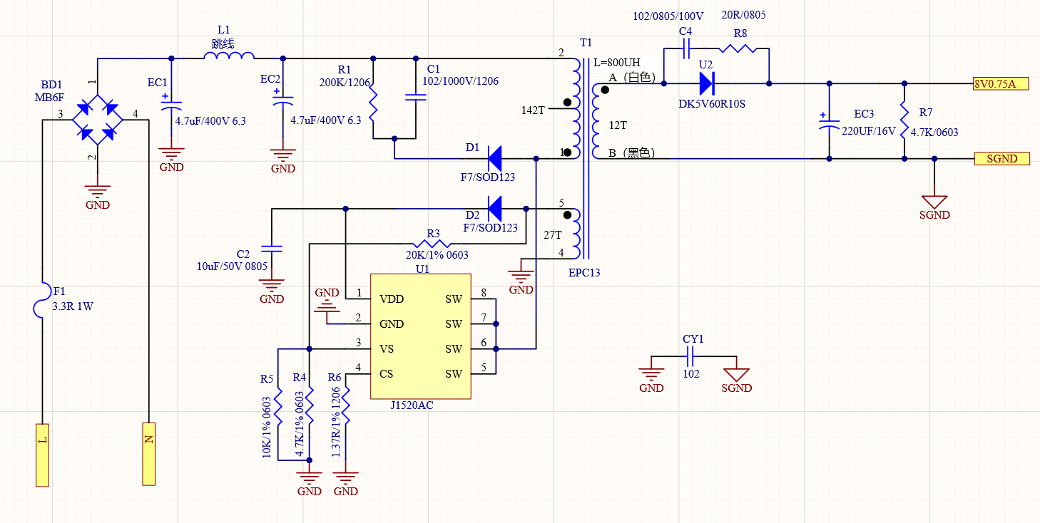
There are many controller IC vendors to choose from for low-power AC-DC supplies. Balancing cost and performance, the JW1520AC from Joulwatt is selected here. The design uses only 21 components in total — extremely simple — and suits the cost-sensitive low-power adapter market where output CV/CC accuracy requirements are not stringent. Key features of the JW1520AC scheme:
- Quasi-resonant (QR) mode reduces switching losses to improve efficiency
- Frequency jitter: ±8% dithering improves EMI
- Standby power as low as 40mW; internal high-voltage startup current source eliminates the startup resistor
- Multi-mode control strategy: QR → PFM → fixed PWM → deep PFM
- PSR control: no optocoupler or secondary feedback circuit needed; CV/CC achieved via auxiliary winding sensing
- Built-in MOSFET: 660V rating, 4.4Ω Rds(on); up to 12W output over the wide AC range
The circuit consists mainly of input rectification/filtering + JW1520AC + EPC13 transformer + synchronous rectification/filtering.
2.3The circuit is very simple — straight to the schematic (example: 8V 0.8A output)
2.4Key Components BOM
| Component | Specification |
|---|---|
| Input fuse resistor | 3.3Ω / 1W (wirewound) |
| Input rectifier bridge | MB6F, 600V / 1A |
| Input E-CAP | 2 × 4.7µF / 400V (rule of thumb ≥ 1.5µF/W) |
| Flyback controller IC | JW1520AC (built-in MOSFET: 660V / 4.4Ω) |
| Output rectifier diode | DFR1M, 1A / 1000V / SOD-123 |
| Flyback transformer | EPC13, Lp = 2mH (see Flyback Transformer Calculation) |
| Secondary SR MOSFET | DK5V60R10S, 60V / 10mΩ |
| Output E-CAP | 220µF / 16V |
2.5Key Power-Device Loss & Thermal Evaluation
The main heat-generating components in this circuit are the input rectifier bridge, switching transistor, transformer, secondary rectifier, etc. Below is the heat estimation method based on this example (input AC90V, output 8V 0.8A); for other output voltages and powers, adjust the parameters and recalculate:
Secondary SR MOSFET: in synchronous rectification conduction loss dominates; switching loss is negligible.
Overall efficiency: 6.4/(6.4+0.9)=87%
Detailed design of the low-cost AC-DC circuit for 10~20W output power
3.1Key Input/Output Specifications
Input voltage: AC100V~AC240V
- Output power Pout
- 10~20W; this example outputs 20W, 16.8V 1.2A
- Output voltage Uout
- DC 3V~30V, regulation accuracy ±1%
- Output current Iout
- 0.1A~4A, CC accuracy ±5%
- Power efficiency Eff
- approx. 86%
- Standby power
- 50~500mW (50mW as a power supply, 500mW as a charger
3.2Overall Circuit Scheme
Balancing cost and performance, the KP22306 from KinYee (BEYLK) is selected here. The design centers on the KP22306 flyback IC with an integrated MOSFET operating in QR mode. With fewer components, it suits the cost-sensitive low-power adapter and battery charger markets. The power circuit mainly consists of AC input rectification/filtering, the KP22306 flyback IC with its RC peripherals, the flyback transformer and the secondary synchronous rectifier; adding op-amp constant current, battery reverse-connection protection and reverse-leakage blocking circuits turns it into a full battery charger. QR mode reduces switching losses and improves efficiency; standby power is as low as 30mW when used as a power supply. The KP22306 built-in MOSFET is rated 650V with 1.7Ω Rds(on), delivering up to 20W over the wide AC range.
3.3The circuit is very simple — straight to the schematic (example: 16.8V CV / 1.2A CC output)
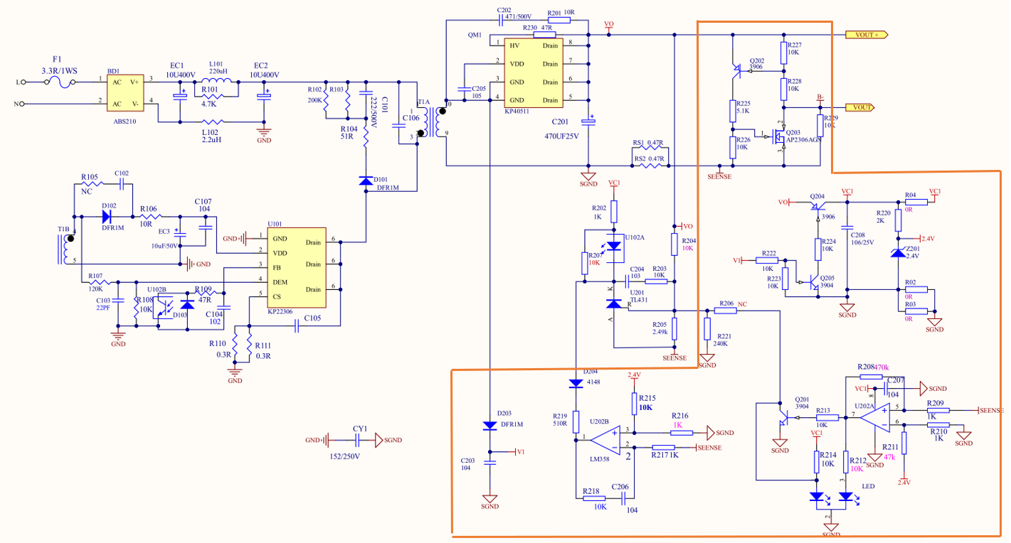
Note: the circuit in the orange box implements the charger functions (constant current, charge-status indication, battery reverse-connection and leakage protection). If only a CV/CC power supply is needed, all components in the orange box can be omitted.
3.4Key Components BOM (example DC16.8V 1.2A output; when output voltage or power differs, some component parameters must be recalculated)
| Component | Specification |
|---|---|
| Fuse resistor | 3.3Ω / 1W (S) |
| Input rectifier bridge | ABS210, 2A / 1kV |
| Input E-CAP | 2 × 10µF / 400V (rule of thumb ≥ 1.5µF/W) |
| EMI differential-mode choke | 22µH (adjust per EMI test results) |
| Isolation optocoupler | EL1018(TA)-VG |
| Flyback transformer | EE1710A, Lp = 650µH |
| Flyback controller IC (integrated) | KP22306A |
| Output E-CAP | 470µF / 25V |
| Synchronous rectifier MOSFET | KP40511SGA (built-in MOSFET, 100V / 16mΩ) |
3.5Key Power-Device Loss & Thermal Evaluation
The main heat-generating components in this circuit are the input rectifier bridge, switching transistor, transformer, secondary rectifier, etc. Below is the heat estimation method based on this example (input AC90V, output 16.8V 1.2A); for other output voltages and powers, adjust the parameters and recalculate:
Overall efficiency: 20/(20+2.39)=89%
Detailed design of the AC-DC circuit for 20~45W output power
4.1Key Input/Output Specifications
Input voltage: AC100V~AC240V
- Output power Pout
- 20~40W; this example outputs 30W
- Output voltage Uout
- DC 2V~60V; this example DC 20V, regulation accuracy ±1%
- Output current Iout
- 0.5A~5A; this example outputs 1.5A
- Power efficiency Eff
- 89%
- Standby power
- 50mW
4.2Overall Circuit Scheme
The design centers on the U8722XX flyback GaN integrated power chip from Union Semiconductor, with an internal GaN HEMT switch operating in QR mode. Using the integrated GaN HEMT chip keeps switching losses low, the external components few and the design simple — suiting the cost-sensitive low-power adapter market with moderate CV/CC accuracy requirements. The U8722DE built-in GaN switch has 0.6Ω Rds(on) with up to 30W output; the U8722EE is 0.48Ω with up to 45W. The power circuit mainly consists of AC input rectification/filtering, the flyback chip and its RC peripherals, the flyback transformer and the secondary synchronous rectifier; adding a PD protocol circuit makes it a PD supply, and adding charger-specific circuits (accurate CC, status indication, battery reverse-connection and reverse-feed protection) completes a full battery charger.
4.3The circuit is very simple — straight to the schematic (example: 30W PD power supply schematic)
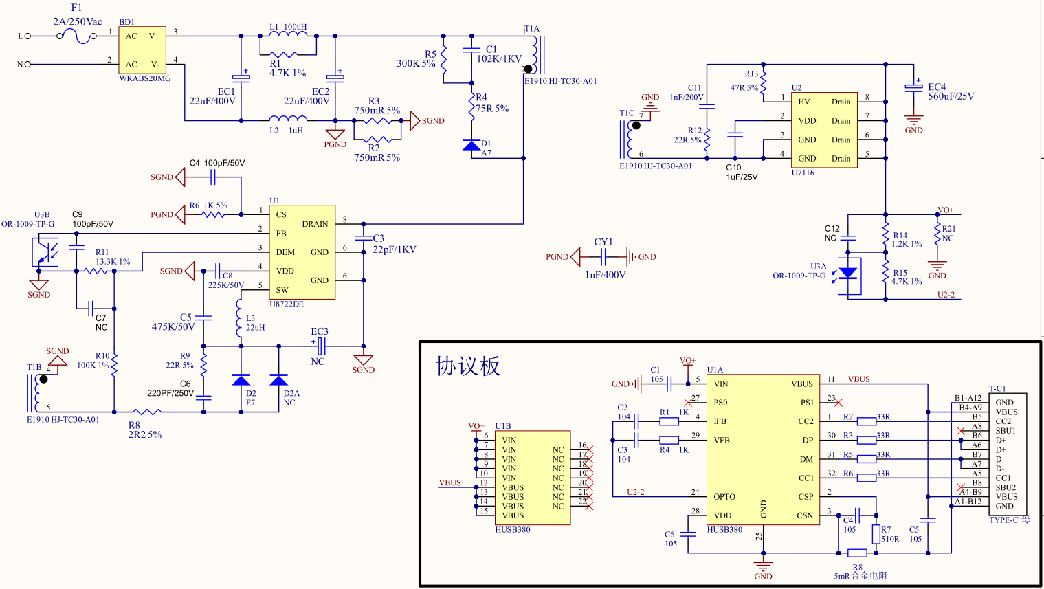
Note: the components in the black box form the PD protocol control circuit. If only a regulated supply is needed, replace the components in that box with a TL431 regulator circuit.
4.4Key Components BOM (example 20V 1.5A output; when output voltage or power differs, some component parameters must be recalculated)
| Component | Specification |
|---|---|
| Fuse | T2A / 250V / slow-blow |
| Rectifier bridge | WRABS20MG, 1kV / 3A |
| Input E-CAP | 2 × 22µF / 400V (rule of thumb ≥ 1.5µF/W) |
| EMI differential-mode choke 1 | 100µH (adjust per EMI test results) |
| EMI differential-mode choke 2 | 2.2µH (adjust per EMI test results) |
| Flyback controller IC | U8722DE, 700V / 0.6Ω |
| Transformer | EC1910B, Lp = 420µH (calculation in Appendix 1 Flyback Transformer Calculation) |
| Synchronous rectifier MOSFET | U7116, 100V / 13mΩ |
| Output E-CAP | 560µF / 25V |
4.5Key Power-Device Loss & Thermal Evaluation
The main heat-generating components in this circuit are the input rectifier bridge, switching transistor, transformer, secondary rectifier, etc. Below is the heat estimation method based on this example (input AC90V, output 20V 1.5A); for other output voltages and powers, adjust the parameters and recalculate:
Overall efficiency: 30/(30+3.33)=90%
Detailed design of the low-cost AC-DC circuit for 45~90W output power
5.1Key Input/Output Specifications
Input voltage: AC100V~AC240V
- Output power Pout
- 45~90W; this example outputs 65W
- Output voltage Uout
- DC 5V~60V; this example DC 20V, regulation accuracy ±1%
- Output current Iout
- 1A~10A; this example outputs 3.25A,
- Power efficiency Eff
- approx. 90%
- Standby power
- approx. 50mW
5.2Overall Circuit Scheme
The design centers on the MK2697 flyback controller IC, operating in QR mode and capable of directly driving an external GaN HEMT switch. Because the GaN HEMT is external, the design is quite flexible. Since AC-DC supplies above 90W must use active PFC to meet safety regulations, the upper power limit of this scheme is set at 90W. The circuit mainly comprises AC input EMI suppression and rectification/filtering, the QR flyback controller and GaN HEMT switch, the power transformer, secondary synchronous rectification and filtering, and the voltage feedback loop. Adding a PD protocol circuit makes it a PD supply; adding charger-specific circuits (accurate CC, status indication, battery reverse-connection and reverse-feed protection) completes a full battery charger.
5.3The circuit is very simple — straight to the schematic (example: 20V CV with 3.5A current limit, rated 65W)
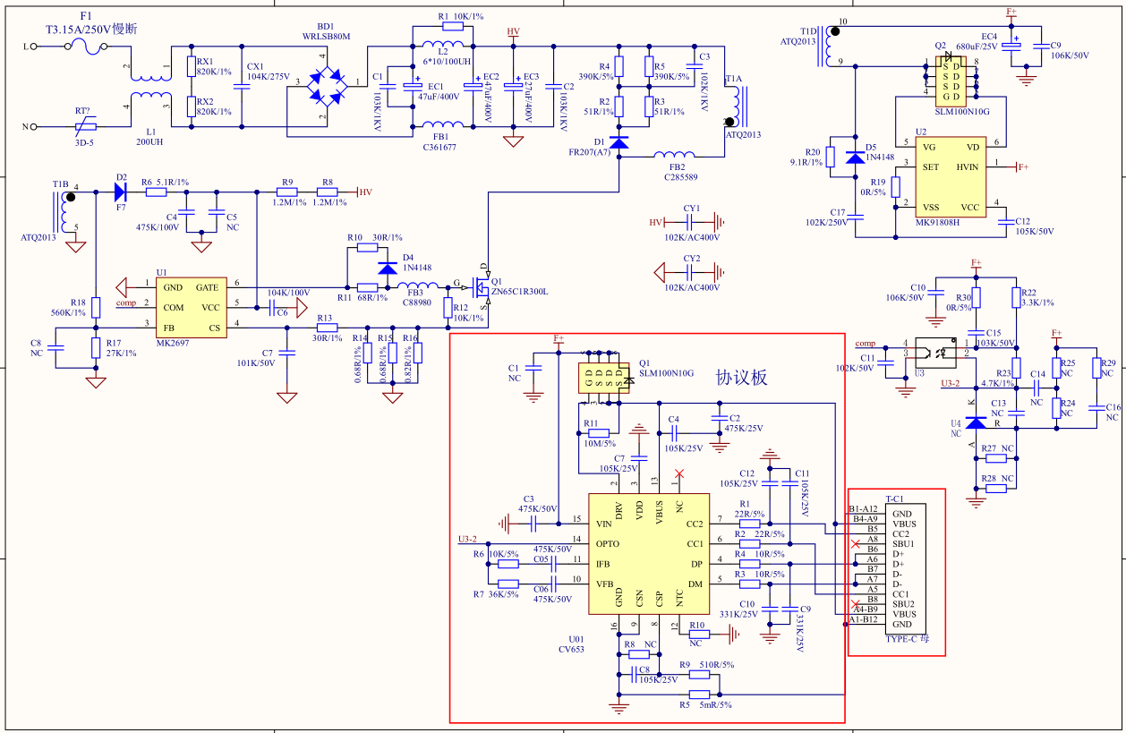
Note: the components in the red box form the PD protocol control circuit and Type-C output port. If only a regulated supply is needed, simply delete the components in the red box.
5.4Key Components BOM (example 20V 3.5A output; when output voltage or power differs, some component parameters must be recalculated)
| Component | Specification |
|---|---|
| Fuse | T2A / 250V / slow-blow |
| Inrush-limiting thermistor | RT10D05, 5Ω |
| EMI common-mode choke | 200µH (adjust per EMI test results) |
| EMI differential-mode cap 1 | X2, 104 / 275V |
| Input AC rectifier bridge | WRLSB80M, 1kV / 5A |
| Input E-CAP | 2 × 47µF / 400V (rule of thumb ≥ 1.5µF/W) |
| EMI differential-mode choke | 100µH (adjust per EMI test results) |
| Flyback controller (QR mode) | MK2697 (directly drives GaN HEMT) |
| GaN switching transistor | ZN65C1R300, 650V / 240mΩ, tf=10ns, Coss=50pF |
| Power transformer | ATQ23.7, Lp = 230µH |
| SR controller IC | KP4060 |
| Synchronous rectifier MOS | SDN10K5P2C, 100V / 13mΩ |
| Output E-CAP | 680µF / 25V |
5.5Key Power-Device Loss & Thermal Evaluation
The main heat-generating components in this circuit are the input rectifier bridge, switching transistor, transformer, secondary rectifier, etc. Below is the heat estimation method based on this example (input AC90V, output 20V 1.5A); for other output voltages and powers, adjust the parameters and recalculate:
Overall efficiency: 65/(65+4.74)=92%