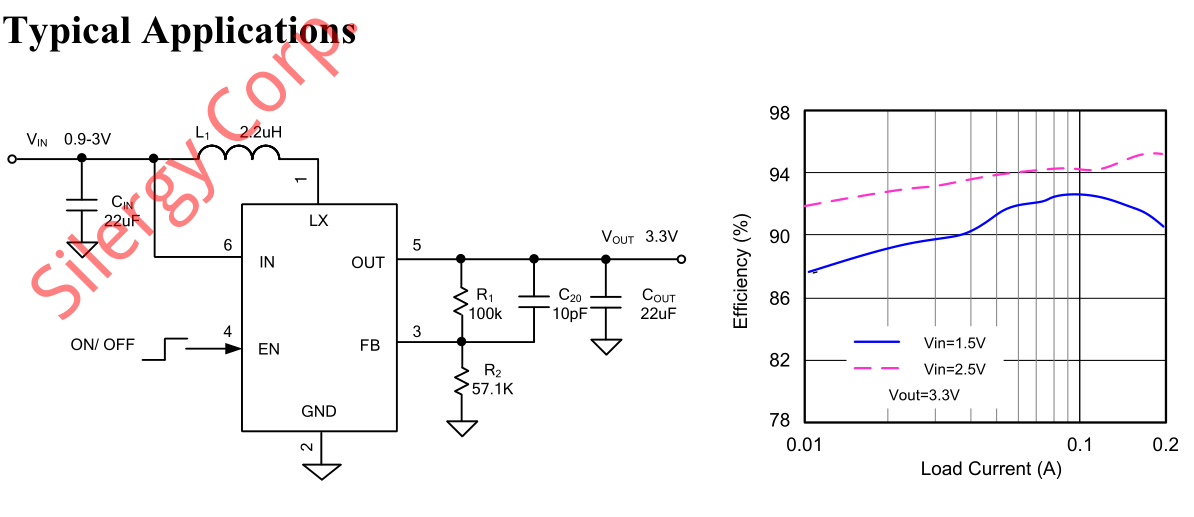
- Boost chip scheme for 1V~5V input, 2~5.5V output:
1.1Scheme: SY7080ABC, 0.9~4V input, 2~4V output, integrated boost chip solution
Input voltage: 0.9V - 4V
- Output voltage
- 2.5V - 4V
- Current limit
- 1.8A
- Switching frequency
- 1.2MHz
Max efficiency: 90% (Vin=1.5V, Vout=3.3V 0.2A)
- Quiescent current
- <1µA
- Rds(on)
- 90mΩ/200mΩ (main/sync)
Inductor: L>=Vin*(Vout-Vin)/(2*Vout*Iout*fs); ensure saturation current > 1.5*Iout
- Capacitors
- ceramic, solid polymer, or high-frequency low-ESR electrolytic
- Chip package
- SOT23-6
- Applications
- portable devices powered by one or two NiMH or alkaline cells.
- Chip reference price
- RMB 1.5
Typical application circuit:
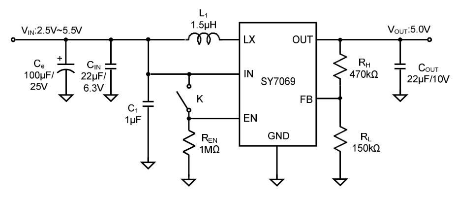
1.2Scheme: SY7069ADC - 1.8V~5V input, 2~5V output, integrated boost chip solution
Input voltage: 1.8V – 5.5V
- Output voltage
- 2.5V – 5.5V
- Current limit
- 3.0A. Note: with TI's TPS61236 the current limit can reach 8A
- Switching frequency
- 1MHz
- Max efficiency
- 94% (Vin=3.6V, Vout=5V 1A); with TI's TPS61236 up to 97%
- Quiescent current
- <1µA
- Rds(on)
- 50mΩ/90mΩ (main/sync)
Inductor: L1= (Vout-Vin)*Vin/(Vout*0.2*Iout*fs); ensure saturation current ≥ 1.2*Iout
- Capacitors
- ceramic, solid polymer, or high-frequency low-ESR electrolytic
- Chip package
- SOT23-6
Applications: single Li-ion cell powered devices, power banks
Chip reference price: RMB 1
Typical application circuit:
- Boost chip scheme for 3V~25V input, 4~25V output:
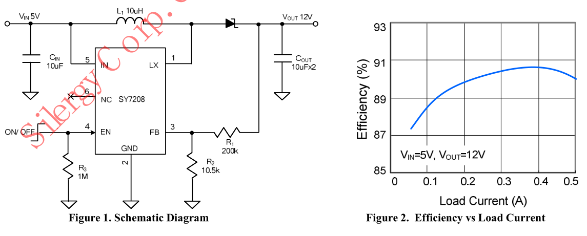
Many vendors offer integrated boost chips in this voltage/current range; here is the cost-effective SY7208ABC:
Chip: SY7208ABC, reference price RMB 1
Input voltage: 3V ~ 25V
- Output voltage
- 4V ~ 25V
- Current limit
- 2.5A. Note: for higher current, TI's TPS61288 with 15A limit is recommended
- Switching frequency
- fixed 1MHz
- Peak efficiency
- >90% (5V input, 12V 0.5A output)
- Quiescent current
- <1µA
- Rds(on)
- 150mΩ
- Chip package
- SOT23-6
- Features
- wide input range, 1µA shutdown current, 1MHz high frequency, built-in 150mΩ MOSFET
- Design case
- 5V→12V/0.5A
Power inductor calculation: L1= (Vout-Vin)*Vin/(Vout*0.2*Iout*fs); note saturation current ≥1.2*Iout
Input/output capacitors: high-frequency low-ESR electrolytic
Applications: automotive devices, industrial control, solar PV, power banks
Typical application circuit:
3General-purpose boost scheme (controller + external MOS)
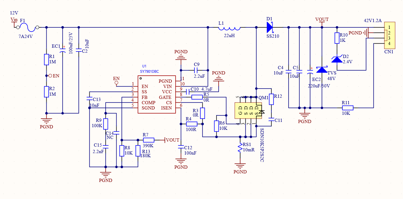
For high-voltage output and other high-current boost circuits, use the general-purpose BOOST scheme below, formed by the SY7901 controller + external MOS:
- Controller
- SY7901DBC, reference price around RMB 2
- Input voltage
- >5V; note the SY7901 supply voltage must not exceed 25V — above 25V use a BUCK stage to power the IC
- Output voltage
- >8V
- Output current
- depends on the external MOSFET.
- Peak efficiency
- 90% (20V input, 40V 2A output)
Features: 500kHz, external MOSFET, no synchronous rectification, complete protection
- MOSFET selection
- Vds>1.3*Vout_max; Rds(on) and switching speed as small as cost allows.
- Power diode
- voltage rating >1.3*Vout, reverse recovery time trr<1/(10*fr), Id>2*Iout
Power inductor calculation: L1= (Vout-Vin)*Vin/(Vout*0.2*Iout*fs); note saturation current ≥1.2*Iout
Input/output capacitors: high-frequency low-ESR electrolytic
Applications: industrial power, chargers, solar PV supply, DC generator supply, etc.
Typical application circuit: