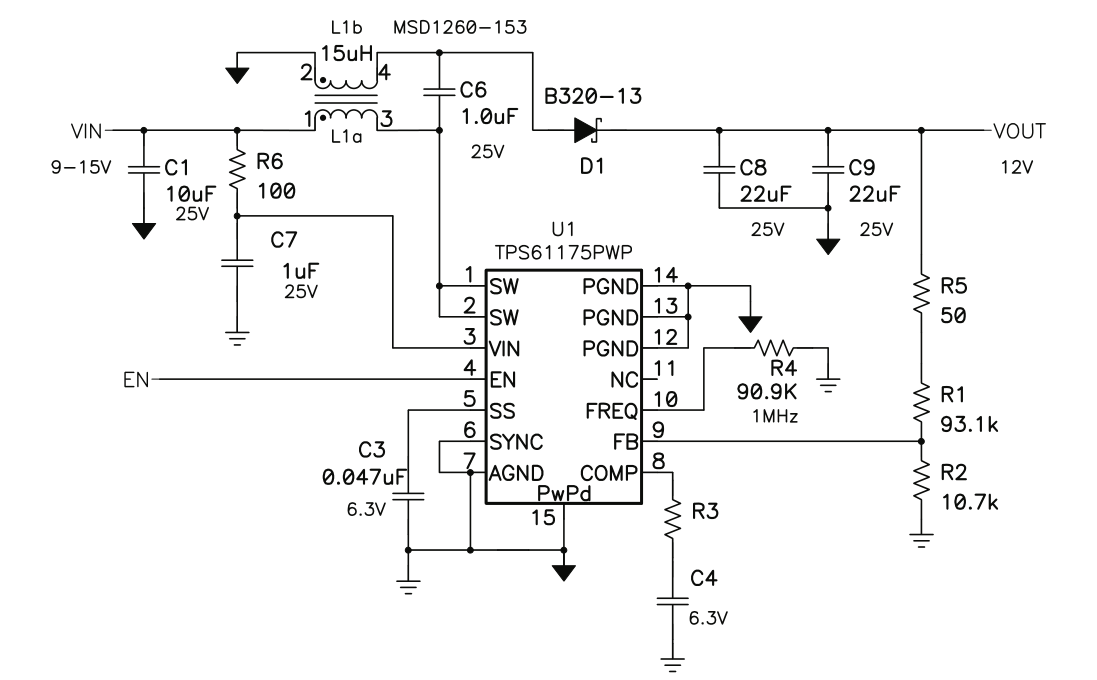
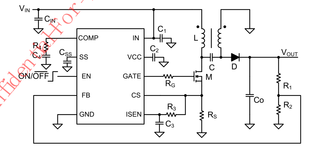
For input below 25V, power below 60W and conversion efficiency not above 90%, the SEPIC scheme is preferred:
- Solution chips
- TI TPS61175 (built-in MOSFET), or Silergy SY7901 (external MOSFET required)
- Input voltage
- 3V ~ 18V/25V (TPS61175 max 18V, SY7901 max 25V)
- Output voltage
- 2V ~ 40V
- Output current
- TPS61175 max 3A, SY7901 max 6A (depends on the external MOSFET)
- Max efficiency
- 90% (12V input, 24V 2A output)
- Operating frequency
- TPS61175 200k~2MHz; SY7901 fixed 600kHz
Features: wide input/output range, automatic buck-boost, simple circuit, small size, complete protection, low cost
Input/output capacitors: ceramic, or high-frequency low-ESR electrolytic
Typical application circuits (TPS61175 and SY7901 respectively):
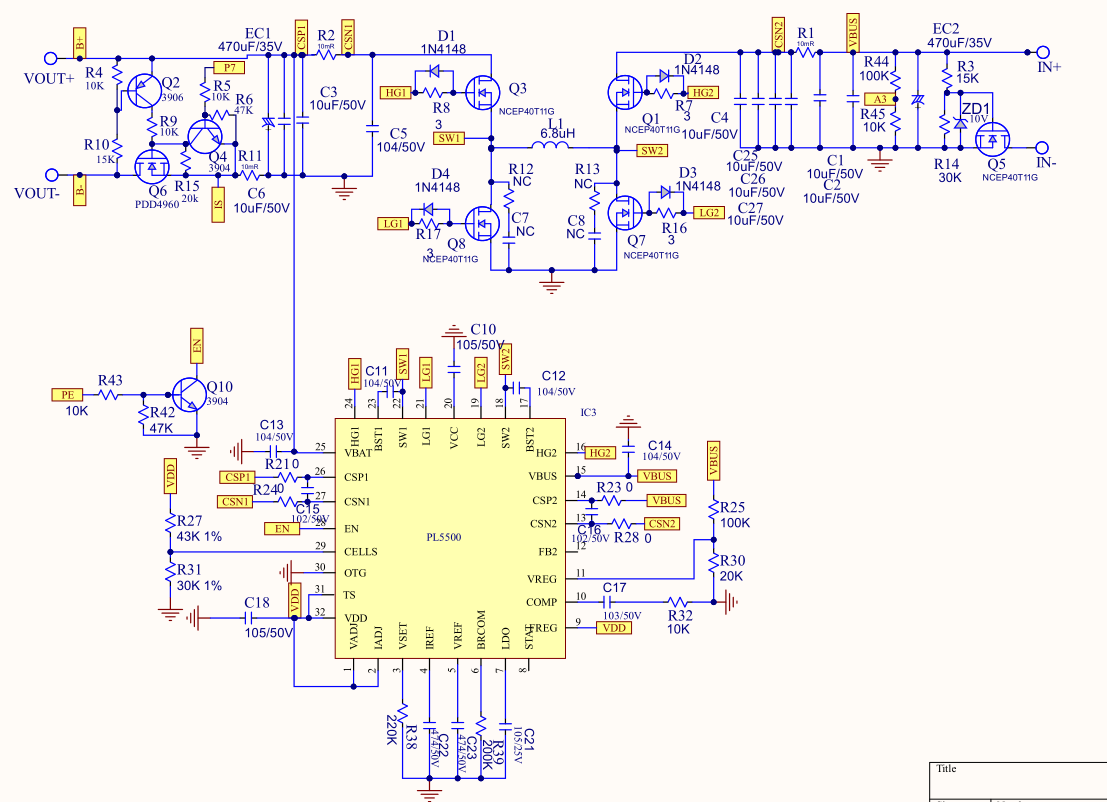
High-efficiency (95%) Buck-Boost scheme for input within 35V and power within 200W:
The four-switch Buck-Boost is the mainstream approach for high-power step-up/step-down; its core advantage is that all four MOSFETs participate in switching, enabling synchronous rectification with efficiency above 95%, and automatic Buck/Boost/mixed mode selection by the Vin/Vout ratio.
Solution chip: PL5501, reference price RMB 6
Input voltage: 4V ~ 36V
- Output voltage
- 3V ~ 36V
- Output current
- max 20A, depends on the external MOSFET
- Switching frequency
- 150kHz ~ 1.2MHz
- Peak efficiency
- >=95% (10~20V input, 16.8V 5A output)
- Chip package
- QFN-32
- Features
- 4-switch synchronous buck-boost topology, complete protection, up to 1.2MHz, supports dynamic adjustment of output vol
tage and current, strong gate drive current (2A), with CC/CV function.
- Design case
- 10~30V input, 16.8V 10A CC/CV output
- MOSFET selection
- Vds>1.5*Vin_max; Rds(on) and switching speed as small as possible; package should aid heat dissipation
- This example uses NCEP40T116
- 40V rating, 3mΩ Rds(on), 5ns rise/fall time
Take the larger of the two
Applications: 12V/24V automotive systems, industrial power, USB PD fast charging and other high-power scenarios
Typical application circuit:
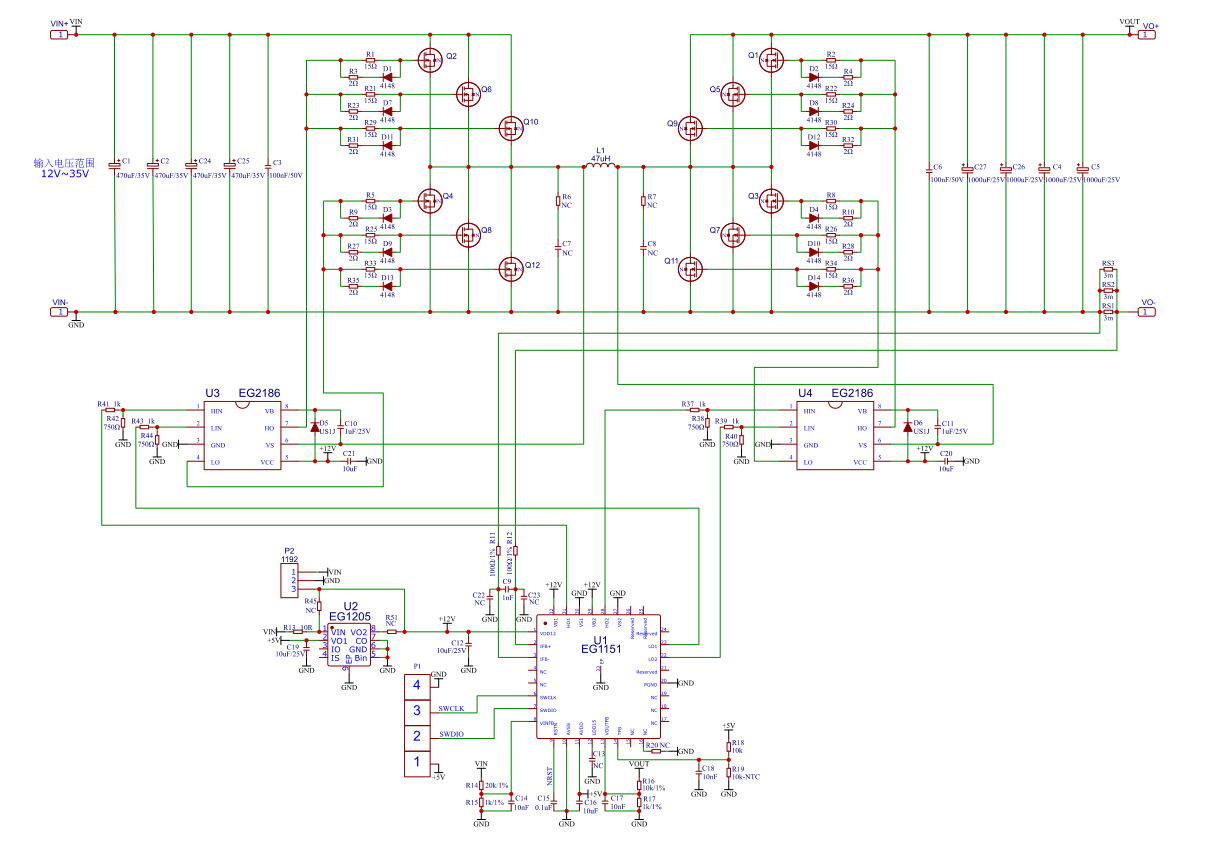
For high power with input or output above 35V, or input below 35V with output power above 200W:
The four-switch Buck-Boost is the mainstream approach for high-power step-up/step-down; its core advantage is that all four MOSFETs participate in switching, enabling synchronous rectification with efficiency above 95%. Chip options for high input voltage are limited; here is EG Micro's EG1151 scheme:
Solution chip: EG1151
Input voltage: 7V ~ 150V
- Output voltage
- 10V ~ 150V
- Output current
- max 20A, depends on the external MOSFET
- Switching frequency
- fixed 70kHz
- Peak efficiency
- >=95% (10~20V input, 16.8V 5A output)
- Chip package
- QFN-32
- Features
- four-switch buck-boost with current-limit and short-circuit protection, MOSFET drive current 1A (slightly
weak; driving high-power MOSFETs needs an external driver IC), maximum voltage rating 150V; suits wide-voltage-range,
high-current buck-boost applications, especially where the voltage is not constant; has CC/CV function.
Design cases: Case 1. 10~100V input, 28V 10A output
Case 2. 10~40V input, 15V 60A output
MOSFET selection: Vds>1.5*Vin_max; Rds(on) and switching speed as small as possible; package should aid heat dissipation
Take the larger of the two
Applications: energy storage, 12V/24V automotive systems, industrial power, portable electronics, etc.
Application circuit 1 (10~100V input, 28V 10A output):
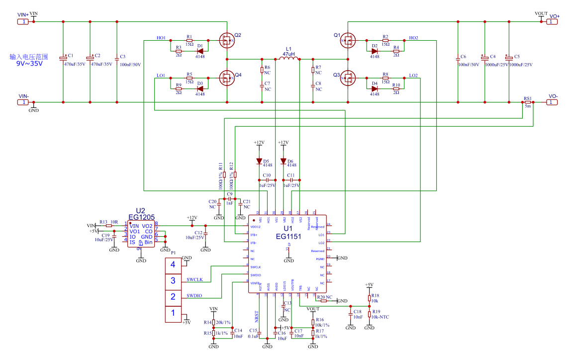
Application circuit 2 (10~40V input, 15V 60A output):