


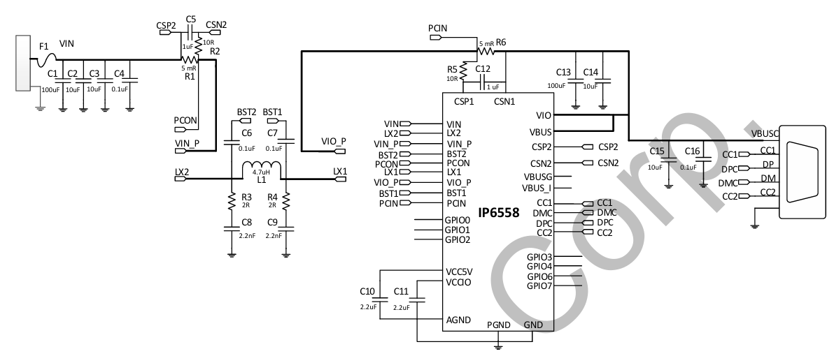
5~30V input, 45W output, single Type-C port: DC input with built-in four-switch synchronous buck-boost converter
Scheme: IP6558. Features
- Built-in four-switch synchronous buck-boost converter, efficiency up to 96%
- Operating input voltage range: 5V to 30V
- Output voltage range: 3V to 20V, auto-adjusted per fast-charge protocol
- Supports 5V, 9V, 12V, 15V, 20V output
- Supports PD2.0/PD3.1, PPS, 3.3V~21V, 20mV/step voltage output
- Supports BC1.2, Apple, AFC, QC2.0/3.0/3.0+/QC4+/QC5
- Supports MTK PE+1.1 and MTK PE+2.0
- Supports FCP, HSCP, AFC, MTK, UFCS
- Multiple protections: input OVP, input UVP, output short circuit, OCP, OVP, OTP
Circuit schematic:
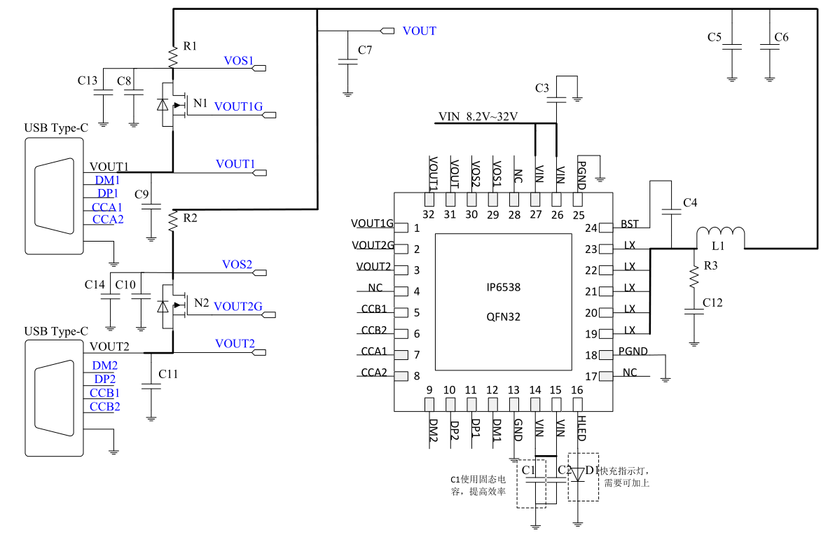
8~32V input, up to 45W output, dual Type-C or C+A ports: single-chip highly integrated DC-input scheme
Scheme: IP6538. Features
- Built-in synchronous buck converter with MOS, efficiency up to 96% (12V–5V 3A)
- Operating input voltage range: 8.2V to 32V
- Output voltage range: 3V to 20V, auto-adjusted per fast-charge protocol
- Supports dual-port fast charging: 2× Type-C or Type-C + A output
- Supports PD3.0 5V, 9V, 12V, 15V, 20V output
- Supports PD2.0/PD3.0 (PPS) and PPS, 3.3V~21V, 20mV/step voltage output
- Supports BC1.2, Apple, AFC, QC2.0/3.0
- Supports MTK PE+1.1 and MTK PE+2.0
- Supports FCP, SCP, SFCP, VOOC
- Multiple protections: input OVP, input UVP, output short circuit, OCP, OVP, OTP
Circuit schematic:
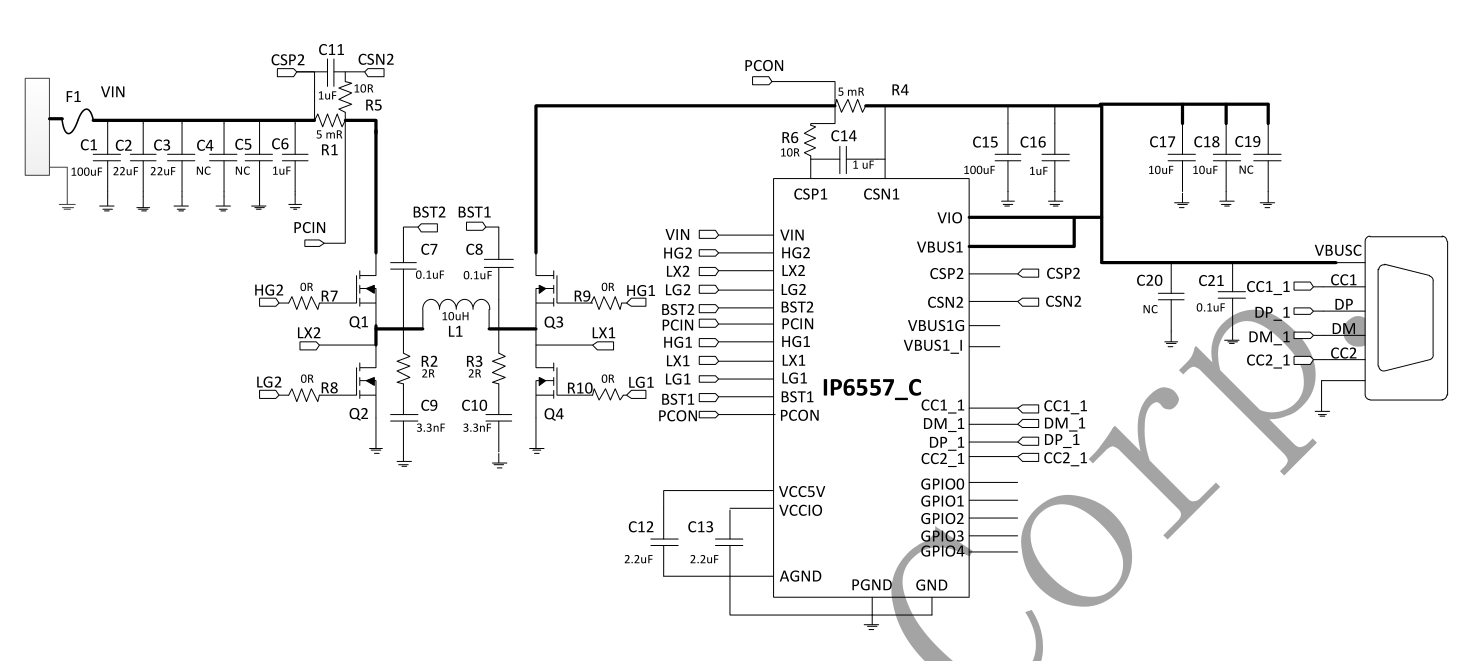
5~31V input, up to 140W output, single Type-C port: single-chip DC-input PD scheme with buck-boost and external MOS
Scheme: IP6537. Features
- Four-switch synchronous buck-boost controller delivering up to 140W (28V 5A),
- 4 external MOSFETs allow flexible device selection and thermal layout
- Supports NTC board-level temperature sensing with intelligent output power adjustment by temperature. Efficiency up to 96%
- Operating input voltage range: 5V to 30V
- Output voltage range: 3V to 28V, auto-adjusted per fast-charge protocol
- Supports 5V, 9V, 12V, 15V, 20V, 28V output
- Supports PD2.0/PD3.1, PPS, 3.3V~21V, 20mV/step voltage output
- Supports BC1.2, Apple, AFC, QC2.0/3.0/3.0+/QC4+/QC5
- Supports MTK PE+1.1 and MTK PE+2.0
- Supports FCP, HSCP, AFC, MTK, UFCS
- Multiple protections: input OVP, input UVP, output short circuit, OCP, OVP, OTP
Circuit schematic:
DC-input PD schemes not covered by items 1~3 above:
For input beyond 5V~31V, or output voltage/power/port count outside items 1~3, use a conventional DC-DC converter (BUCK, BOOST or BUCK-BOOST) plus a PD protocol controller:
If input is below 5V, refer to Boost Circuit Design + PD Power Secondary-Side Circuit Design.
If input is above 30V, refer to Buck Circuit Design + PD Power Secondary-Side Circuit Design.
For other cases refer to Buck-Boost Circuit Design + PD Power Secondary-Side Circuit Design.