


Forward AC-DC Power Circuit Features:
Forward AC-DC supplies usually take AC100~240V input, with recommended output power of 150~500W, output voltage DC 0~90V and current up to 50A. A forward circuit's output voltage can be continuously adjustable from zero volts. If the output voltage is fixed or varies only within a small range (±15%), the 150W~500W range is now generally implemented with a half-bridge LLC, since it offers higher efficiency without a significant cost increase.
The forward topology splits into single-switch and two-switch schemes. The single-switch scheme is relatively simple, needing only 1 switch and 1 reset winding, but the switch endures 2× input voltage stress, requiring high-voltage devices (e.g. 800V+ MOSFETs); efficiency is modest and it suits low-cost small-power applications below 150W — now progressively replaced by AHB flyback circuits. In the two-switch scheme both switches turn on simultaneously; diodes automatically clamp the switch voltage to the input level, halving the voltage stress so lower-rated devices can be used. It is highly reliable with relatively small switching losses, and with secondary synchronous rectification efficiency can easily exceed 90%, with maximum power above 500W.
Detailed design of the 150~500W continuously-adjustable-output AC-DC supply:
Key Input/Output Specifications:
Input voltage: AC100V~AC240V
- Output power
- 150-500W; this example 200W; see the difference table for other outputs
- Output voltage
- DC 0~100V; this example 0-5V continuously adjustable, regulation accuracy ±1%
- Output current
- 0~50A; this example 0~40A continuously adjustable, current accuracy ±5%
- Power efficiency
- 85~92% (varies with output voltage)
- Standby power
- 1~5W (varies with the number of functions)
Overall Circuit Scheme
The power circuit adopts a "PFC + two-switch forward + synchronous rectification" architecture for high efficiency and high power density. The front-end PFC uses the L6562A controller in boundary conduction mode to improve input power quality and meet energy-efficiency regulations. The power conversion stage is a two-switch forward topology controlled by the NCP1252AD, offering good core reset capability and generous switching stress margin — suitable for efficient medium-power applications. The output uses the SP6019S8RGB synchronous rectifier control IC to greatly reduce secondary rectification loss and raise overall efficiency. Voltage and current are sampled through precision op-amps and fed to CV/CC comparators, enabling wide-range voltage and current adjustment. Since the system has many functional units, a separate auxiliary power supply powers each unit.
Block diagram of the main circuit units and the power circuit diagram:
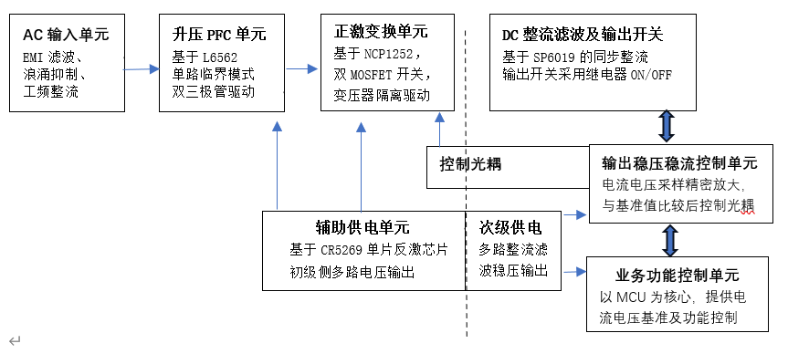
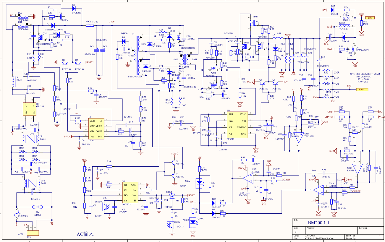
Detailed Description of Each Circuit Unit
AC input unit (EMI filtering, rectification, surge suppression): single-phase AC three-wire input (line L, neutral N, ground G). After fuse F1, varistor RV1 absorbs surge spikes; the EMI filter uses LF1/LF2 two-stage differential-mode chokes, two differential X2 capacitors and four Y-connected Y-capacitors, followed by rectifier bridge BD1 and a differential-mode filter formed by L1 and CB1/CB2. This circuit supports up to 600W.
PFC unit: the circuit is mainly a boost topology consisting of the PFC boundary-mode controller U1 (L6562A), switch QM1, power diode D1 and power inductor T4, boosting the rectified DC to a stable high DC voltage (380V). The control mode is critical conduction mode (CrM), where the inductor current stays at the boundary between continuous and discontinuous in every switching cycle, reducing switching losses. At lower output power the minimum frequency can be set to 70~80kHz; at higher power, e.g. 400~500W, it can drop to 40~60kHz. Because CrM resets the inductor flux to zero every cycle, a ferrite transformer core is chosen.
Two-switch forward conversion unit: the circuit consists of the NCP1252AD controller U3, two switches QM2/QM3, drive transformer T1, main power transformer T2, two diodes D5/D6 and related peripherals. When both main switches conduct, input voltage Vin is applied to the transformer primary winding and energy is transferred to the secondary, where synchronous rectification supplies the load and the output inductor/capacitor; when both switches turn off, the primary magnetizing current cannot change abruptly and flows back naturally to the input capacitor through the two clamp diodes, completing natural magnetic reset.
DC output synchronous rectification and output switch control unit: composed of the synchronous rectifier with its spike-absorbing RC, the synchronous driver IC, energy-storage inductor, freewheeling switch, electrolytic storage/filter capacitors, output relay switch and voltage/current sampling RC networks. The synchronous control IC is the SP6019S8RGB, a digitally controlled drain-source voltage sensing synchronous rectifier controller. The relay can immediately cut off the output when necessary (e.g. output short circuit or a shutdown command from the MCU).
CV/CC control unit: this unit usually consists of 4 op-amps and a primary-secondary feedback optocoupler, including two control loops — one for voltage regulation and one for current regulation. The two loops are isolated by a diode so that whichever is lower, output voltage or output current, takes effect, achieving automatic switching between CV and CC modes. The CV or CC reference comes from the MCU main control unit, RC-smoothed and fed to the op-amps; both voltage and current samples are first amplified by precision op-amps before going to the comparators for regulation control.
2.5. Key Components BOM List
| Component | Specification |
|---|---|
| Slow-blow fuse | T5A / 250V |
| Surge-limiting varistor | 10D471 |
| Common-mode choke 1 | 2mH / 5A |
| X2 capacitor | 2 × 0.47µF / 275V |
| Common-mode choke 2 | 10mH / 5A |
| Y2 capacitor | 2 × 10²M / 400V |
| Input AC rectifier bridge | 800V / 15A |
| EMI differential-mode choke | 100µH / 5A (wire dia. 0.8mm, T18×9×6.5mm toroid, 40 turns) |
| PFC inductor | 160µH (PQ2625 core) |
| PFC diode | 10A / 600V (fast recovery diode) |
| Primary high-voltage E-CAP | 68µF / 450V |
| PFC main switch | HCS60R150S (tf=18ns, Rds(on)=0.18Ω, Coss=50pF) |
| PFC controller | L6562A (boundary mode) |
| Main transformer | PQ3225 |
| Forward main switch | HCS60R150S (tr=23ns, tf=18ns, Rds(on)=0.18Ω, Coss=50pF) |
| Demagnetizing diode | 600V / 4A (ultrafast recovery) |
| Forward controller | NCP1252AD |
| Synchronous rectifier MOSFET | PDP0980 (4.2mΩ, tr=tf=40ns) |
| Forward energy-storage inductor | 8µH / 40A (Sendust toroid) |
| Output E-CAP | 2200µF / 10V |
| Synchronous rectifier IC | SP6019S8RGB |
| Precision op-amp | TP1282L1 |
2.4.6Key Power-Device Loss & Thermal Evaluation
The main heat-generating components are the input filter rectifier bridge, the magnetic components of the PFC and forward converters, power switches and power rectifiers. Below is the heat estimation method based on this example (input AC100V, output 5V 40A); for other output voltages and powers, adjust the parameters and recalculate:
(The upper and lower switches of the two-switch forward are in series, so their losses are equal; per switch:
Total power loss:
Overall efficiency: 200/(200+37)=84.4%